
If computer chips make the modern world go around, then Nvidia and TSMC are flywheels keeping it spinning. It’s worth paying attention when the former says they’ve made a chipmaking breakthrough, and the latter confirms they’re about to put it into practice.
At Nvidia’s GTC developer conference this week, CEO Jensen Huang saidNvidia has developed software to make a chipmaking step, called inverse lithography, over 40 times faster. A process that usually takes weeks can now be completed overnight, and instead of requiring some 40,000 CPU servers and 35 megawatts of power, it should only need 500 Nvidia DGX H100 GPU-based systems and 5 megawatts.
“With cuLitho, TSMC can reduce prototype cycle time, increase throughput and reduce the carbon footprint of their manufacturing, and prepare for 2nm and beyond,” he said.
Nvidia partnered with some of the biggest names in the industry on the work. TSMC, the largest chip foundry in the world, plans to qualify the approach in production this summer. Meanwhile, chip designer, Synopsis, and equipment maker, ASML, said in a press release they will integrate cuLitho into their chip design and lithography software.
What Is Inverse Lithography?
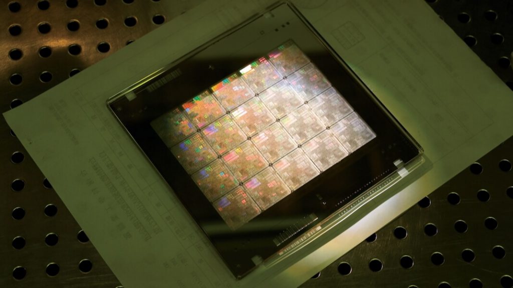
To fabricate a modern computer chip, makers shine ultraviolet light through intricate “stencils” to etch billions of patterns—like wires and transistors—onto smooth silicon wafers at near-atomic resolutions. This step, called photolithography, is how every new chip design, from Nvidia to Apple to Intel, is manifested physically in silicon.
The machines that make it happen, built by ASML, cost hundreds of millions of dollars and can produce near-flawless works of nanoscale art on chips. The end product, an example of which is humming away near your fingertips as you read this, is probably the most complex commodity in history. (TSMC churns out a quintillion transistors every six months—for Apple alone.)
To make more powerful chips, with ever-more, ever-smaller transistors, engineers have had to get creative.
Remember that stencil mentioned above? It’s the weirdest stencil you’ve ever seen. Today’s transistors are smaller than the wavelength of light used to etch them. Chipmakers have to use some extremely clever tricks to design stencils—or technically, photomasks—that can bend light into interference patterns whose features are smaller than the light’s wavelength and perfectly match the chip’s design.
Whereas photomasks once had a more one-to-one shape—a rectangle projected a rectangle—they’ve necessarily become more and more complicated over the years. The most advanced masks these days are more like mandalas than simple polygons.
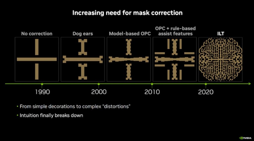
To design these advanced photomask patterns, engineers reverse the process.
They start with the design they want, then stuff it through a wicked mess of equations describing the physics involved to design a suitable pattern. This step is called inverse lithography, and as the gap between light wavelength and feature size has increased, it’s become increasingly crucial to the whole process. But as the complexity of photomasks increases, so too does the computing power, time, and cost required to design them.
“Computational lithography is the largest computation workload in chip design and manufacturing, consuming tens of billions of CPU hours annually,” Huang said. “Massive data centers run 24/7 to create reticles used in lithography systems.”
In the broader category of computational lithography—the methods used to design photomasks—inverse lithography is one of the newer, more advanced approaches. Its advantages include greater depth of field and resolution and should benefit the entire chip, but due its heavy computational lift, it’s currently only used sparingly.
A Library in Parallel
Nvidia aims to reduce that lift by making the computation more amenable to graphics processing units, or GPUs. These powerful chips are used for tasks with lots of simple computations that can be completed in parallel, like video games and machine learning. So it isn’t just about running existing processes on GPUs, which only yields a modest improvement, but modifying those processes specifically for GPUs.
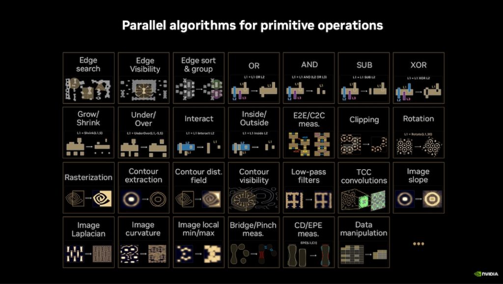
That’s what the new software, cuLitho, is designed to do. The product, developed over the last four years, is a library of algorithms for the basic operations used in inverse lithography. By breaking inverse lithography down into these smaller, more repetitive computations, the whole process can now be split and parallelized on GPUs. And that, according to Nvidia, significantly speeds everything up.
“If [inverse lithography] was sped up 40x, would many more people and companies use full-chip ILT on many more layers? I am sure of it,” said Vivek Singh, VP of Nvidia’s Advanced Technology Group, in a talk at GTC.
With a speedier, less computationally hungry process, makers can more rapidly iterate on experimental designs, tweak existing designs, make more photomasks per day, and generally, expand the use of inverse lithography to more of the chip, he said.
This last detail is critical. Wider use of inverse lithography should reduce print errors by sharpening the projected image—meaning chipmakers can churn out more working chips per silicon wafer—and be precise enough to make features at 2 nanometers and beyond.
It turns out making better chips isn’t all about the hardware. Software improvements, like cuLitho or the increased use of machine learning in design, can have a big impact too.
Image Credit: Nvidia
Author: Jason Dorrier
Jason is editorial director of Singularity Hub. He researched and wrote about finance and economics before moving on to science and technology. He’s curious about pretty much everything, but especially loves learning about and sharing big ideas and advances in artificial intelligence, computing, robotics, biotech, neuroscience, and space.